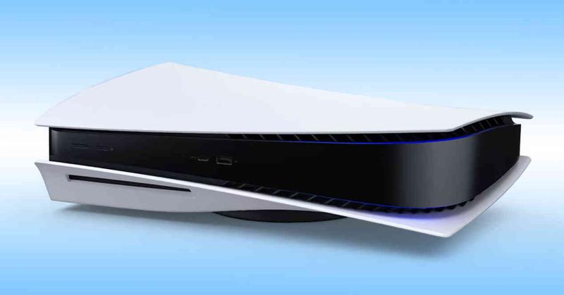
The PS5 is Sony’s fifth home console, successor to the best-selling console in the seventh generation of consoles, where Sony’s console ended up winning the game over Microsoft’s. Sony, like Microsoft, has once again relied on AMD for PlayStation 5 to make use of its technologies, but with a different point of view where, despite using the same technologies, the Sony console has its own personality.
The new Sony console, unlike Microsoft’s, is presented in two different models on the market.
The first model with a cost of 400 euros lacks the BluRay reader and is called Digital Edition, so it can only play games in digital form. The second is the standard PlayStation 5 that has this type of reader and costs $ 100 more. In the case that you have PlayStation 4 games in disc format, the standard version is recommended to be able to play the games of the previous generation that you have in disc format.
The PlayStation 5 SoC
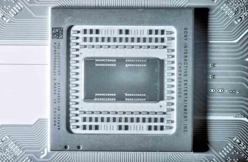
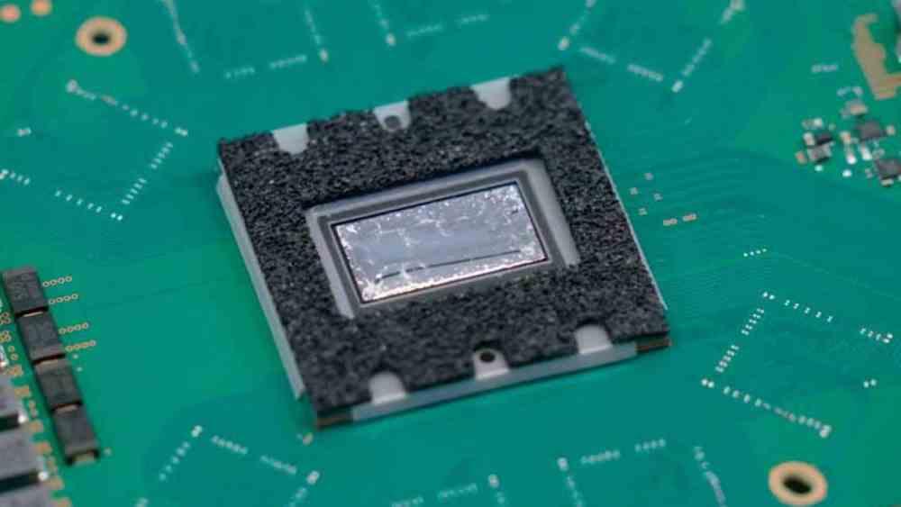
The PlayStation 5 SoC is a chip that integrates all the elements of the system into a single processor except for the RAM, SSD storage, I / O interfaces and the flash memory controller. It is a custom SoC made by AMD for Sony, so its organization is unique despite using parts already seen on PC.
This SoC is between the Xbox Series S and the Xbox Series X in size, since it is smaller than that of Microsoft’s most powerful console, which measures 360 mm 2 , while that of the PS4 is close to the 300 mm 2 . In part this is explained by the configuration of its GPU and certain cuts in the CPU cores that we will discuss in this post.
It should be noted that since the launch of the original PlayStation 4, Sony has been cutting the total area of its new SoCs with each new iteration. The reason for this we do not know, but it is something that draws powerfully attention that we can assign to an attempt to get a greater number of chips per wafer and therefore more consoles for sale if we look at the full glass or due to the fact that Sony economically it has no muscle to hold a more expensive SoC, if we look at the empty glass.
The PlayStation 5 CPU
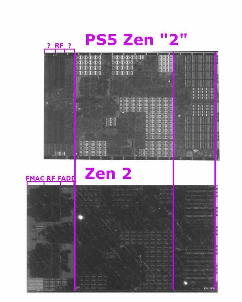
The CPU of the new Sony console like those of Microsoft is based on Zen 2, but it is a slightly shortened version, since AMD at Sony’s request has cut the set of registers for floating point in half. The consequence of this is that you cannot execute the AVX-256 instructions in a single instruction cycle but in at least two instruction cycles. Therefore, its vector floating point capacity is more similar to Zen than to Zen 2. In any case, we cannot fall into the error of thinking that it is a Zen 1 despite having this feature cut out.
Another cut in the cores is the removal of the FADD drive. In each Zen 2 core there are two types of units in charge of doing floating point additions, which are FADD and FMAC, the latter being capable of performing addition and multiplication in an instruction cycle. For the purpose of adding only, the FADD unit takes 3 cycles while FMAC takes 5 clock cycles.
Out of the rest of the omissions, the rest of the CPU is exactly the same as the Zen 2 of the “Renoir” type of the AMD Ryzen 4000 and both Xbox Series in terms of performance.
PS5 GPU, RDNA 2 custom again

| Base architecture | AMD RDNA 2 custom |
|---|---|
| Base clock speed | 800MHZ (PS4 mode), 911MHz (PS4 Pro mode) |
| Boost clock speed | 2.23 GHz |
| Compute Units | 36 |
| ALUs FP32 by CU | 64 |
| Power in FP32 | 10.23 TFLOPS |
| Power in FP16 | 21.46 TFLOPS |
| Power in Int 8 | – |
| Texture Units | 144 |
| Texturing rate | 321.12 Gtéxels / s |
| ROPS | 64 |
| Fill Rate | 142.72 GPixels / s |
| Cache L2 | 4 MB |
| Mesh / Primitive Shaders | Yes |
| Variable Rate Shading | Not |
| Ray tracing | Yes |
| Sampler Feedback Streaming | Proprietary solution |
| Infinity Cache | Not |
The PlayStation 5 GPU is about the same as seen on the RX 6700 XT, but with 4 of the 40 Compute Units idle, so Sony’s contrary to the jump from 40 units to 52 from the Xbox One to the Xbox Series X have decided to keep the number of Compute Units from PS4 Pro to PS5. Of course, we have gone from GCN to RDNA 2, or at least RDNA 2 Custom if we take into account the words of Mark Cerny in his presentation “Road to PS5”.
The RDNA 2 Custom concept together with the fact that Sony has given almost no data on certain details of the internal hardware of the console have created doubts about whether the GPU is RDNA 2 or RDNA 1. The origin of this? The PlayStation 5 SoC began to be rumored under the names Ariel, Oberon, and Flute in their various stages of pre-production and SoC design. All codenames are related to William Shakespeare’s play A Midsummer Night’s Dream and at that time the codename Navi 10 Lite was related to the PlayStation 5 SoC, i.e. RDNA 1.
It was Mark Cerny’s presentation where it helped us to be clear that the GPU is an RDNA 2, at least they told us about Ray Tracing support. What is the addition of the Ray Acceleration Units, which in RDNA 2 are integrated into the texture units. However the addition of RAUs seems to be a last minute change in the final hardware. At the end of the day they only needed to change the unit of textures on the original design.
Notable absences in the PS5 GPU
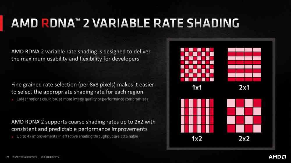
The biggest absence of the GPU is the Variable Rate Shading, which is a way to save resources when applying the Pixel Shader. The idea of the VRS is to locate the lines of instruction that are exactly the same both in opcode and the data of the same, to unify them in a single calculation instead of repeating them repeatedly.
To apply this, the RDNA 2 for PC and Xbox have had to renew the Render Backend units, which are what we call ROPS in a GPU. Where AMD traditionally separates them into Z-ROPS and Color ROPS. Well, on PS5 they are the same as RDNA and not those of RDNA 2. The same can be said of the rasterized unit, which is also RDNA. The consequences? The lack of support for Variable Rate Shading by hardware, although it is possible to do it by software.
What is the speed of the PS5 GPU?
Sony, unlike Microsoft, has not opted for a design with more Compute Units, but they have increased the GPU clock speed to 2.23 GHz, but the counterpart is that this clock speed does not reach 100% of the time. The reason for this is that Sony, unlike Microsoft, has decided to adopt AMD’s SmartShift technology, which means having variable clock speeds in both CPU and GPU.
The idea of the SmartShift is that CPU and GPU share the same energy “environment”, where it is possible that when the CPU does not have a very high workload it becomes possible to increase the clock speed of the GPU and vice versa. Sony has not given the CPU and GPU performance profiles, but we do know the maximums for both CPU and GPU.
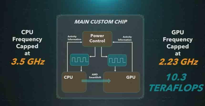
It must be taken into account that in the SoCs much lower clock speeds are reached in their components than with these separately, the proximity of the components makes it little recommended that the maximum clock speeds be reached. With the Smartshift it is possible to place the GPU at 2.23 GHz at certain times.
The fact that SONY has chosen this option makes us think that the SoC of their console was already finished with a lower power and they had no time for it to return to the design table. Had they taken a path with more Compute Units, this would have delayed the SoC from six months to a year, affecting the launch of the console, which would give Microsoft a year ahead in the market.
RAM on PlayStation 5
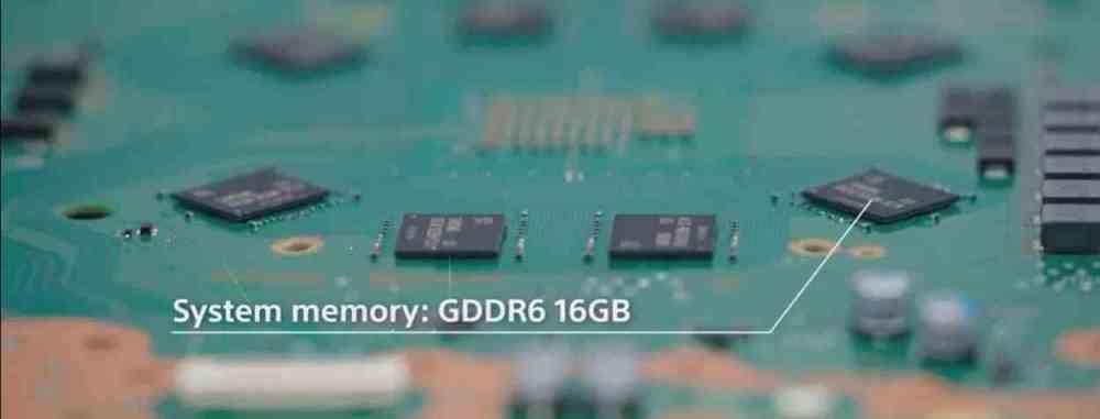
PlayStation 5 has 16 GB of GDDR6 RAM, divided into 8 chips of 2 GB each connected through a 256-bit bus to the SoC where each is GDDR6 14 Gbps, so we are facing a configuration at 448 GB / s of bandwidth. Sony has not reported memory bandwidth data separately like Microsoft, which may be a different approach to memory access or the same approach.
- Approach # 1: The same as the Xbox Series X, but we do not know which parts of the RAM are exclusive to the GPU and which are shared between the CPU and GPU.
- Approach # 2: Both CPU and GPU share the same memory space in RAM.
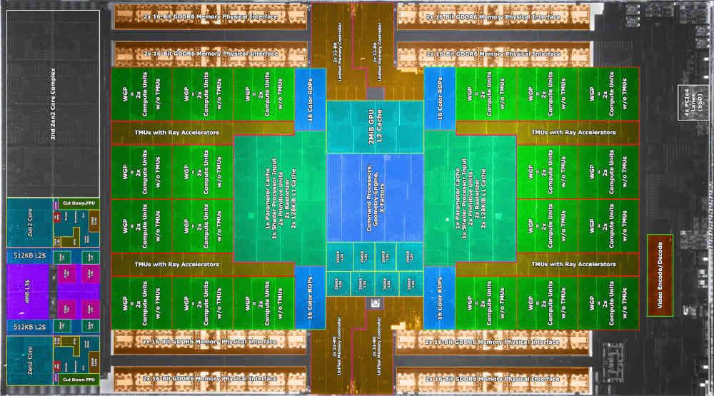
Looking at the SoC of the console it is not very clear to us which of the two options Sony has made for its new console. The advantage of the Microsoft method is that there is no contention when accessing memory by two clients on the same channel, the other method does create contention in access, since when a RAM memory is in a single channel has two clients the sum of the bandwidths of both clients is less than the total bandwidth.
The PS5 custom SSD Controller
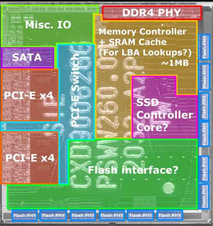
SONY has bet very strongly on the issue of storage for the SSD, although it is not a unique feature in this generation, unlike Microsoft where the controller of its SSD has been made by a third party, in PS5 it is a controller made to measure that actually serves two functions:
- As an SSD controller.
- Like Southbridge of the system.
In the second case it is related to the DDR4 memory chip, which is next to the SSD controller, its usefulness? PS5, like its predecessor, has a Southbridge that in stand-by mode of the console runs another operating system that allows it to manage downloads when we have the console in sleep mode. Obviously, that operating system needs a RAM to work and hence the DDR4.
As Southbridge also integrates a series of input and output interfaces such as the SATA controller for the UHD BluRay reader
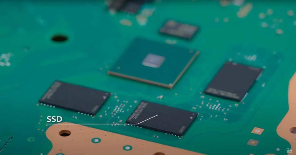
As for the internal SSD of the console, we have 6 NVMe memory chips on the board located on the front and back of it. Each of the NVMe chips assigned to 2 of the 12 channels of the flash controller and with a capacity of 128 GB of storage each. SONY talks about 825 GB of storage, but it really is 768 GB from the moment they have counted from 1000 to 1000 instead of 1024 to 1024. So we are facing a storage that is 3/4 of that of the Xbox Series X, but at a much higher speed.
Contrary to both Xbox Series, here we have the four PCI Express 4.0 lanes assigned to the SSD controller, which communicates with the system SoC under a real speed 5.5 GB / s bus. It must be taken into account that new generation consoles have real-time compression and decompression mechanisms that allow compressed data to be transmitted on the same 5.5 GB bus at a rate of 9 GB / s.
Storage expansion
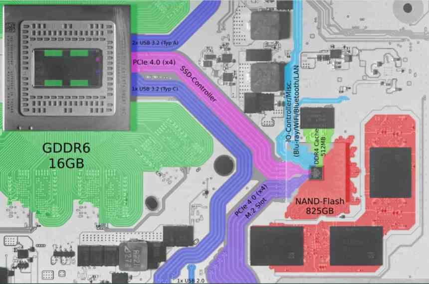
SONY, contrary to Microsoft, has decided to opt for standard M.2 cards for PCs of various sizes, although in the first months of the console’s life, the console and the list of M.2 units with which the console is cannot be updated. compatible is unknown at the time of this writing.
The dual PCI Express 4.0 x4 interface on the SSD controller is what attracts the most attention, since the external SSD does not communicate with the SoC directly but with the SSD controller, this means that the flash memory controller that is in the M.2 drive if it is faster than the PS5 it will not exceed it in speed. On the other hand, it also makes it possible to launch cheaper M.2 discs for PlayStation 5 without the flash controller or SSD.
When it comes to expanding the storage of the console, we are faced with a cheaper option than in the Xbox Series to be able to use M.2 units for PC, but the counterpart comes from the fact that expanding is much more complex than in Microsoft consoles.

